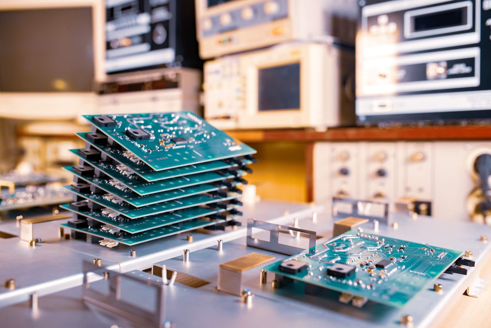
Quality assurance is of paramount importance when you invest in printed circuit board or PCB assembly. One malfunctioning connection or a faulty element may cause an electronic device that is priced high to go to waste, result in expensive recalls and lost reputations.
Testing is more than a luxury in PCB manufacturing- it is your insurance policy against field failures and customers complaints. Today electronics require accuracy at the microscopic scale, and any minor fault can propagate into system-wide issues. Knowledge of different testing methodologies in the market can guide you to make wise choices in regards to quality control and your products should meet the standards of the industry.
1. In-Circuit Testing (ICT)
In-circuit testing is the gold standard of individual component verification of assembled PCBs. This technique involves a bed-of-nails contactor to contact a given test point with electrical contact to enable technicians to independently measure resistance, capacitance and other electrical characteristics of each component.
ICT is very efficient in discovering defects in manufacturing like parts omission, wrong part values and even soldering problems. It can be used to ensure that resistors are within their measured values, capacitors are operating within tolerance and integrated circuits are getting the correct power supply voltages.
Nevertheless, ICT demands dedicated fixtures per PCB design and is only cost-effective to use with large production runs. Initial equipment cost may be big, and the unit testing cost is insignificant at high quantities.
2. Functional Testing
Functional testing is the other method used to test the PCB assembly and it involves how well the PCB executes its role as a full system. This approach does not focus on the individual components but uses the power to the board and confirm that the results of the inputs are equal to the expected outputs.
This type of testing is very similar to the operating conditions in the real world, thus is great at identifying problems in a system that component-level testing cannot identify. Communication protocols, signal timing and overall system performance can be checked by means of functional tests.
The difficulty is in the creation of test procedures which test all the functions of the circuits with reasonable test time. Functional tests that are well-designed provide a balance between full coverage and efficiency in manufacturing.
3. Automated Optical Inspection (AOI)
The AOI systems incorporate high-resolution cameras and an advanced image processing algorithm to scan PCB assemblies to detect visual defects. Such systems are able to identify missing parts, wrong orientations, soldering flaws and placement errors at extremely high speeds and accuracy.
Modern AOI machines are faster than lightning and can test a complete board within seconds missing the faulty components that could escape the attention of human inspection. The technology is very efficient in detecting blatant manufacturing mistakes before they are subjected to costly testing.
AOI is also not efficient; it should be used with other methods of testing since it does not check the functionality of the electrical. Other flaws, e.g. internal component failures, or marginal solder joints, cannot be detected by optical inspection.
4. Flying Probe Testing
Bed-of-nails ICT cannot match the flexibility that is provided by flying probe testing. Rather than predetermined test points, this technique employs moving probes, which can reach any almost any point on the PCB under the control of a computer.
This method does not require costly custom fixtures and so it is best used in prototype testing and in low volume production. Flying probe systems are capable of making most of the electrical tests that ICT achieves and responding rapidly to design modifications.
This trade-off is the speed of testing, with the probes being physically moved between the test points. This renders flying probe testing less appropriate in the high-volume manufacturing process where throughput is the most important factor.
5. Boundary Scan Testing
Boundary scan testing uses in-built tests that are built into present-day integrated circuits. According to this IEEE 1149.1 standard, external test equipment can gain control and monitor the inputs and outputs of conforming ICs with as little as a four-wire interface.
The technique is especially useful in the test of complicated digital circuits whose physical layout makes probe access hard or inaccessible. Boundary scan is able to identify stuck-at faults, interconnection opened and shorts between ICs.
This is limited by the compatibility of the components i.e. devices that have internalized the boundary scan feature can only be used in this form of testing. Boundary scan testing, however, is becoming more powerful as more manufacturers add this feature.
Conclusion
The choice of PCB assembly testing techniques is determined by a wide range of factors: volume of production, complexity, cost based, and quality targets. Several manufacturers use several testing strategies in series, whereby quicker methods such as AOI are used as a first-line screening test and followed by more intense electrical tests.
ICT and AOI are the two automated systems that are usually used in high-volume production when prototypes and small batches are being tested with flying probe testing and functional verification. The trick is to ensure that testing capacity is aligned to manufacturing process with appropriate cost-efficiency.
Take your unique needs into consideration i.e. a solid testing strategy will identify defects at the initial stage, minimize field failures and finally ensure your brand image stays intact in a market that is becoming very competitive.
If you are looking for a fine PCB assembly manufacturer, look no further than OptimaTech Inc.